Difference between revisions of "Dio breakout"
Jump to navigation
Jump to search
(Created page with "thumb|300px|alt=The DIO breakout board|The DIO breakout board. This is the documentation page for the DIO_breakout . == Overview == This board en...") |
(→Pinout) |
||
| Line 27: | Line 27: | ||
The connector at the bottom of the board is laid out as follows: |
|||
{| border=1 |
{| border=1 |
||
! pin !! function |
! pin !! function |
||
| Line 47: | Line 48: | ||
|} |
|} |
||
the power-connector at the top of the board is laid out as follows: |
|||
{| border=1 |
{| border=1 |
||
| Line 68: | Line 71: | ||
|} |
|} |
||
The dataconnector in the middle of the board is compatible with the DIO board: |
|||
{| border=1 |
|||
! pin !! function |
|||
|- |
|||
| 1 || GND |
|||
|- |
|||
| 2 || VCC |
|||
|- |
|||
| 3 || IO0 |
|||
|- |
|||
| 4 || IO1 |
|||
|- |
|||
| 5 || IO2 |
|||
|- |
|||
| 6 || IO3 |
|||
|- |
|||
| 7 || d.n.c. |
|||
|- |
|||
| 8 || IO4 |
|||
|- |
|||
| 9 || IO5 |
|||
|- |
|||
| 10 || IO6 |
|||
|} |
|||
== jumper settings == |
== jumper settings == |
||
Revision as of 15:19, 17 May 2013
This is the documentation page for the DIO_breakout .
Overview
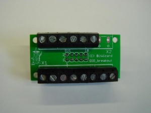
This board enables use screw terminals to connect wires to your SPI_DIO or I2C_DIO board.
Assembly instructions
None: the board comes fully assembled.
External resources
Datasheets
Additional software
Related projects
Pinout
The connector at the bottom of the board is laid out as follows:
| pin | function |
|---|---|
| 1 | GND |
| 2 | IO0 |
| 3 | IO1 |
| 4 | IO2 |
| 5 | IO3 |
| 6 | IO4 |
| 7 | IO5 |
| 8 | IO6 |
the power-connector at the top of the board is laid out as follows:
| pin | function |
|---|---|
| 1 | GND |
| 2 | VCC |
| 3 | GND |
| 4 | VCC |
| 5 | GND |
| 6 | VCC |
| 7 | GND |
| 8 | VCC |
The dataconnector in the middle of the board is compatible with the DIO board:
| pin | function |
|---|---|
| 1 | GND |
| 2 | VCC |
| 3 | IO0 |
| 4 | IO1 |
| 5 | IO2 |
| 6 | IO3 |
| 7 | d.n.c. |
| 8 | IO4 |
| 9 | IO5 |
| 10 | IO6 |
jumper settings
There are no jumpers.
Future hardware enhancements
Future software enhancements
Changelog
1.0
- Initial public release
