Difference between revisions of "USB-multio"
| Line 5: | Line 5: | ||
== Overview == |
== Overview == |
||
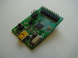
The USB-Multio PCB has an USB connector and a 20-pin IO connector. The brains of the PCB is an at90usb162 (or compatible) chip. |
The USB-Multio PCB has an USB connector and a 20-pin IO connector. The brains of the PCB is an at90usb162 (or compatible) chip.<br> |
||
The USB-Multio PCB can be bought in the [http://www.bitwizard.nl/shop/avr-boards/usb-multio-21 BitWizard shop]. |
|||
== Assembly instructions == |
== Assembly instructions == |
||
Revision as of 13:18, 2 November 2015
This is the documentation page for the USB-Multio PCB.
Overview
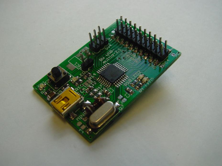
The USB-Multio PCB has an USB connector and a 20-pin IO connector. The brains of the PCB is an at90usb162 (or compatible) chip.
The USB-Multio PCB can be bought in the BitWizard shop.
Assembly instructions
The USB-Multio PCB can be configured in multiple ways, depending on the application. A variety of is included, to suit most needs.
Possible configurations
Directly plugged into breadboard
Solder the golden, round headers on the outer two rows of holes. Don't use regular headers, they will ruin your breadboard!
We prefer so let these pins stick down, so the board is mounted om the breadboard, with the microcontroller visible. It is of course possible to mount the pins on the other side, but mounting the SPI/ISP or RESET header, would then make it impossible to plug the multio into a breadboard.
Connected with 20p ribbon cable
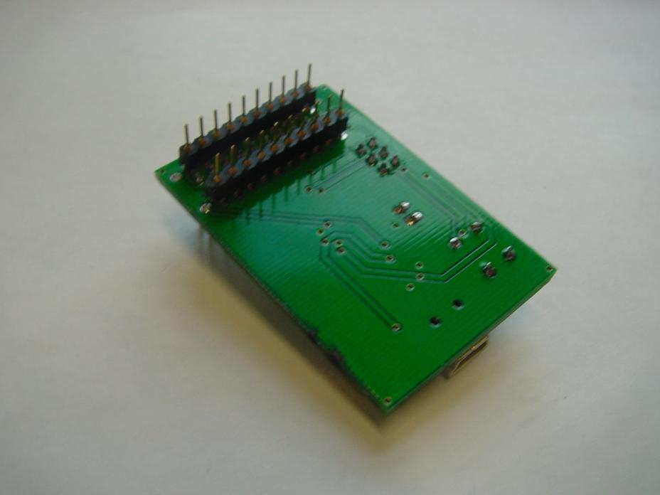
Solder the 2x10 header in the middle of the 4x10 hole array, on the same side as all the other components. If you solder the header on the other side, the pin numbering as listed below will no longer be correct. On the other hand, if you have a similar board with 2x10 female connectors on top, you'd be able to plug it into that other board just like that!
Connected to RGB_clock PCB
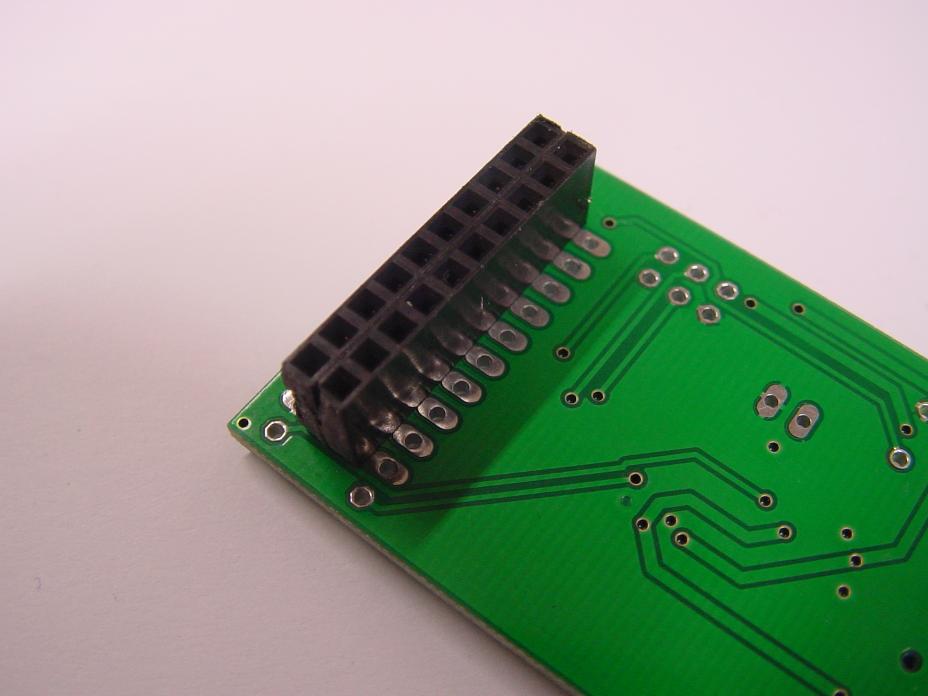
Solder the two female header strips on the bottom side of the PCB, in the middle of the 4x10 hole array.
External resources
Datasheets
Additional software
For software development, implmenting USB communication we recommend LUFA:
Related projects
Example projects
Pinout
The 20 pin connector is connected as follows
| 1 | GND |
| 2 | GND |
| 3 | PD1 (AIN0 / INT1) |
| 4 | PD2 (AIN1 / RXD1 / INT2) |
| 5 | PD3 (TXD1 / INT3) |
| 6 | PD4 (INT5) |
| 7 | PD5 (XCK1 / PCINT12) |
| 8 | PD6 (/RTS / INT6) |
| 9 | PB1 (SCLK / PCINT1) |
| 10 | PB0 (/SS / PCINT0) |
| 11 | PB3 (PDO / MISO / PCINT3) |
| 12 | PB2 (PDI / MOSI / PCINT2) |
| 13 | PB5 (PCINT5) |
| 14 | PB4 (T1 / PCINT4) |
| 15 | PB7 (OC0A / OC1C / PCINT7) |
| 16 | PB6 (PCINT6) |
| 17 | PC6 (OC1A / PCINT8) |
| 18 | PC7 (ICP1 / INT4 / CLKO) |
| 19 | VCC |
| 20 | VCC |
- rx PC5
- tx PC4
JP1 is connected in parallel with the reset button, to provide an external reset header.
PC4 and PC5 are also brought out to solder pads, next to the 20-pin connector.
LEDs
Version 2.1
- led1 is connected to VCC
- led2 is connected to PD0
- led3 is connected to PC2
- led12 is connected to PD7
Version 2.0
- led1 (near the bottom) is connected to PC2
- led2 (near the AVR) is connected to PD0.
Jumper settings
Version 2.1
| SJ1 | SJ2 | IC1 | |
| 5V | 1 | 0 | NOT mounted |
| 3V3 <50mA | 0 | 1 | NOT mounted |
| 3V3 >50mA | 0 | 0 | mounted |
0 Means open, 1 means bridged.
JMP1: ICSP-Enable. CAUTION! Pin 1 and 2 are connected by a narrow PCB track. Cut this if you want to change this jumper setting.
1-2: Default: SS connected to pin PB0 (MCU can function as an SPI slave or master, or as an ICSP programmer)
2-3: ICSP enabled, SS connected to reset (programming the MCU over the 6-pin connector is enabled)
Use as a programmer
The usb-multio can be used as a programmer for ICSP programming other Atmel processors.
For this you need the AVRISP software from http://www.fourwalledcubicle.com/AVRISP.php
This has not been tested yet.
programming
This section describes how you get your program into the processor.
In general what you need to know is that the processor will boot into the code you programmed into it on powerup. Once you're done developing your program, that's the way you'll use it: Powerup, run.
If there is no program loaded or if you press the reset button the chip comes up in "firmware upload mode". This is done by a bootloader. You should take care not to overwrite or erase the bootloader, because there is no way to put the bootloader back once it is gone.
Linux
Get the dfu-programmer for atmel chips package. (link?)
On sufficiently recent Ubunu distributions that is as simple as:
sudo apt-get install dfu-programmer
I recommend creating a script called "dfu":
#!/bin/sh
if [ -z "$CHIP" ]  ; then
  chip=at90usb162
else
  chip=$CHIP
fi

hex=$1
sudo dfu-programmer $chip erase
sudo dfu-programmer $chip flash --suppress-bootloader-mem $hex
sudo dfu-programmer $chip start
TODO: figure out how to get rid of the "sudo" commands here...
Now downloading and starting a program is as simple as pressing the reset button and then:
dfu <yourbinary>.hex
TODO: When I'm developing, I'm likely to modify the code, and when I want to program the chip I hit the "reset" button on the board. Then the computer will see my chip re-enumerate as the Atmel DFU chip. A simple script could watchout for that and invoke dfu <mycurrentbinary>.hex the moment the chip has enumerated. Once that's running downloading and starting the latest code becomes as simple as hitting the reset button.
Apparently the FLIP program is now available for Linux too. See below.
Windows
Get the "flip" program from Atmel. http://www.atmel.com/dyn/products/tools_card.asp?tool_id=3886
If you prefer a commandline tool, Atmel provides a program called BATCHISP.EXE that comes with the FLIP package.
Writing programs
The chip is an at90usb162. http://www.atmel.com/dyn/resources/prod_documents/doc7707.pdf
You can program the processor as if it is a normal AVR processor without USB. Just like an arduino. Or you can program it to have USB support. For this the LUFA package is very useful. http://www.fourwalledcubicle.com/LUFA.php
Depending on what you want you can start from these examples:
DONE: Find out if we can jump to the bootloader from our code so that we can issue a "go get yourself updated" command over the USB (yes, but the documentation says nothing about what address to jump to). This comes in handy if the reset button is difficult to reach because the device is built-in somewhere. http://www.atmel.com/dyn/resources/prod_documents/doc7618.pdf
Physical dimensions
2.1
Board outline: 50x34 mm(1.97x1.32 inch)
2.0
Future hardware enhancements
- Make sure that all pins with special functions are exported to the connector.
- Make a header for all pins not provided on the external connector.
- Make an I2C header
Future software enhancements
- program the LUFA bootloader.
- Program an even smaller bootloader. (512 bytes should be possible, CF teensy/halfkay).
Changelog
2.1
- Removed row of 8 resistors + LEDs
- Added ICSP connector
- Added jumper for external reset
- Added possibility to mount connector, to directly plug the board into a breadboard.
- Added pads for PC4 and PC5
- Connected extra LED to PD7
2.0
- Initial public release


