Stmwifi
This is the documentation page for the STMWIFI board.
Overview
The board has a connector for an ESP8266 WIFI module, an USB port and a bunch of IO connectors.
Assembly instructions
None: the board comes fully assembled.
Specifications
The FET outputs on the "ODO" pins are capable of sinking about 1A per output. We have tested 1A and the FET became slightly warm, as predicted by theory.
Although the specifications for the FETs allow a larger current, it is not recommended to exceed the 1A max we specify.
Possible Configurations
We recommend powering the board through an USB connector.
Currently the firmware does not yet support enumerating as an USB device. This should become available in the future.
The "console" of the device is currently on the connector called "UART". Connect a TTL-level usb-serial device there. The baud rate is 115200.
The J2-J6 connectors provide an easy way to connect three-pin-sensors. For example DHT11, DHT22, or DS18S20. Future firmware may support using the connectors as a servo output. The pinout is prepared for servos: 1-GND, 2-VCC, 3-signal. The signal pins are connected to PA4, PA5, PA7, PA8, PB1 respectively.
the SV3 connector provides 16 GPIO pins. These are connected to GPIOC.
The ODO (I don't remember what that stands for) connector provides VCC (5V or 3.3V), GND and 4 open drain outputs. You could drive a 5-pin stepper with this, or a led strip. There is no flyback diode, so if you're driving inductive loads, you should provide one yourself.
The chip has two I2C modules that are brought out to an I2C connector. You might be able to use these as GPIO or more sensors too. No real firmware support for I2C yet.
The SPI bus is brought out to the SPI connector. The pinout is the same as for AVR ICSP connectors (and documented elsewhere on this wiki). The firmware currently initializes the SPI module, and allows sending text to the BitWizard SPI LCD modules.
External resources
Datasheets
- The STM32F072 datasheet: http://www.st.com/st-web-ui/static/active/en/resource/technical/document/datasheet/DM00090510.pdf
- The STM32F0x2 reference manual: http://www.st.com/st-web-ui/static/active/en/resource/technical/document/reference_manual/DM00031936.pdf
Additional software
Related projects
Pinout
For the SPI connector see: SPI_connector_pinout.
For the I2C connector see: I2C_connector_pinout.
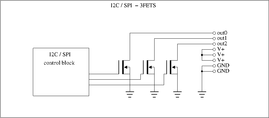
The output connector is connected as follows:
| pin | function | |
|---|---|---|
| 1 | OUT0 | |
| 2 | OUT1 | |
| 3 | OUT2 | |
| 4 | V+ | |
| 5 | V+ | |
| 6 | V+ | |
| 7 | GND | |
| 8 | GND |
The "V+" is a convenience connector. The GND of your powersupply needs to be connected to GND, and your load goes between the plus of your powersupply and the "OUT" signals. You could wire it directly from the powersupply, or you can connect the powersupply to the "V+" here, and the loads between another V+ and the OUTx connector.
This board does not provide a protection diode between the OUTx signals and V+. This allows you to connect say a 5V powersupply to V+ and use OUT1 and OUT2 for 5V devices, while you connect a 12V load between OUT0 and a 12V powersupply. (the protection diode would allow the 12V powersupply to feed the 5V line through the 12V load and the protection diode when the 12V load was meant to be off.)
The MOSFETs that we use are specified to be able to handle an inductive kickback. This means they will survive an occasional inductive spike, but not when you trigger that too often, say by putting the output in PWM mode.
So, if you have an inductive load you will need to provide your own protection diode, especially if you're going to use the PWM mode.
LEDs
The only LED is a power-LED.
Block diagram
Here is a block diagram of the board.
Power connector
Jumper settings
See solder jumpers on how to change the solder jumper.
By changing the solder jumper SJ1, you can make the connector nearest the board edge into the ICSP programming connector for the attiny44 on the board.
