FT4222h
This is the documentation page for the FT4222h breakout board. That you can buy in the BitWizard shop.
overview
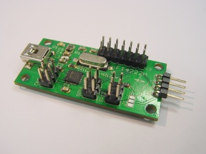
The FT4222h breakout board has an USB connector, two SPI connectors, one I2C connector one CNF connector and one 14-pin IO connector. The brains of the PCB, of course, is an FT4222h chip.
External resources
pinout
See SPI connector pinout for the pinout of the SPI connectors.
As you might expect, the two SPI connectors share the SCK, MISO and MOSI signals to the FT4222H. The slave select on the two SPI connectors route to "SSO0" and "SS"
On the I2C connector you can find the I2C signals SDA (pin 2) and SCL (pin 3) as well as GND (pin 1) and VCC (pin 4). There is no pullup on the i2c lines on the board. You have to provide that externally.
The power (VCC pin) on the I2C and SPI connectors can be jumper selected between 5V and 3V3. The 5V comes from the USB connection. It should be assumed to be limted to 500mA, whereas the 3.3V comes from the FT4222H itself. The datasheet does not specify how much current can be drawn. If you use this to power "slave" circuits, you must verify that you're not drawing too much yourself. (Keep in mind that the 3.3V regulator inside the FT4222H is meant to power just the FT4222H. FTDI often specifies "not for external use" or "max 10mA", but I could not find that in THIS datasheet).
The 14 pin connector at the top has the following pinout:
- 1 - GND
- 2 - GND
- 3 - SCL
- 4 - SDA
- 5 - GPIO2
- 6 - GPIO3
- 7 - MOSI
- 8 - MISO
- 9 - IO2
- 10 - IO3
- 11 - SCK
- 12 - SS0O
- 13 - +3.3V
- 14 - +5V.
On the SPI and I2C connectors there is a pin called "VCC". The voltage is selectable between 5V and 3.3V. Note that even if you select 5V, the io signals still go directly into the chip which is meant to work with 3.3V voltage levels. (the chip could also work with 1.8 or 2.5V IO signal levels, but on this board it is not configured like that).
LEDS
- The only LED is a power LED
Jumper settings
The FT4222H chip provides a low-power 3.3V output voltage. You can chose to provide that 3.3V or the 5V from the USB on the SPI and I2C connectors.
In the picture here, the jumper to select between 3.3V and 5V is still a solder jumper. I've since found that I change such more often than is practical with a solder jumper, so I've decided to change it to a real jumper. When the jumper is 1-2, near the edge of the PCB, the VCC is configured 3.3V, and when the jumper is 2-3, near the middle of the PCB VCC is configured for 5V (from USB).
The CNF jumpers allow you to configure the DNCFx signals on the FT4222H. Put the jumper near you (if the USB is on the left) for a 0 and away from you for a 1.
DCNF1 is on the left, DCNF0 is on the right.
| DCNF1 | DCNF0 | mode | num interfaces |
|---|---|---|---|
| 0 | 0 | mode 0 | 2 |
| 0 | 1 | mode 1 | 4 |
| 1 | 0 | mode 2 | 4 |
| 1 | 1 | mode 3 | 1 |
please refer to FTDI documentation about the available option in each of the modes.
Usage
To use the board/chip, you can download the FT4222H library from FTDI's product page. It is available for Linux, Windows and Mac.
future hardware enhancements
Changelog
1.1
- Initial public release
