Difference between revisions of "I2C splitter"
| Line 36: | Line 36: | ||
== Power jumper/power connector == |
== Power jumper/power connector == |
||
If your board has a jumper labeled "VOUT" near the bottom, this can be used to select the voltage level on the output bus. Connect a jumper on the rightmost two pins (AUX/VCC) to use the power from the "master" connector on the left or right of the PCB. If that is undesired, for example if your slave devices are 3.3V, you can connect a 3.3V power source to the ground pin on the left and the VAUX pin in the middle. |
If your board has a jumper labeled "VOUT" near the bottom, this can be used to select the voltage level on the output bus. Connect a jumper on the rightmost two pins (AUX/VCC) to use the power from the "master" connector on the left or right of the PCB. If that is undesired, for example if your master is 5V and your slave devices are 3.3V, you can connect a 3.3V power source to the ground pin on the left and the VAUX pin in the middle. |
||
= using the board = |
= using the board = |
||
Revision as of 14:55, 3 June 2015
general info
Based on the PCA9548A chip from NXP
http://www.nxp.com/documents/data_sheet/PCA9548A.pdf
I2C address:
1110 000 tru 1110 111 (jumper selectable)
Each I2C output has 4K7 pull-up resistors.
The address would be written "0x70" for the Linux I2C-tools. BitWizard "naming convention" would call this address "0xe0".
physical dimensions
- Board outline: 50x25mm
- Mounting hole diameter: 3mm
- Mounting hole pitch: 44x19mm (3mm from board edge)
pinouts
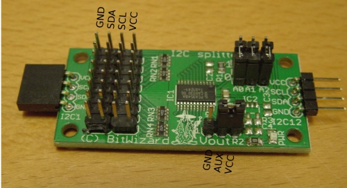
Hold the board such that the 4x8 pin array is on the left.
The 4x8 array has from left to right, GND (labeled "V-" because "GND" didn't fit), SDA (labeled DA), SCL (CL), and VCC (V+).
From top to bottom you will find bus 0 at the top to bus 7 at the bottom.
Connect your "master device" to the connector on the left or right. The pinout is GND, SDA, SCL, VCC from bottom to top.
The "Vout" connector provides GND/AUX/VCC. By placing a jumper on AUX/VCC, you can configure your slave I2C busses to use the same power supply as your main VCC (usually 5V or 3.3V). If you require a different voltage, you can apply that voltage using a two-pin connector using GND/AUX on the same connector. If you ordered the special version prepared for a specific output voltage, no connection/jumper is necessary on the VOUT connector. You can measure the output voltage on the AUX pin if you want (there are 8 other pins that make this voltage available, but it's there. :-) )
jumpers
address jumpers
It is recommended you use address 0 for the PCA9548A, unless that clashes with something on your I2C bus. Put all three jumpers to the position nearest you, in the position marked "0".
Power jumper/power connector
If your board has a jumper labeled "VOUT" near the bottom, this can be used to select the voltage level on the output bus. Connect a jumper on the rightmost two pins (AUX/VCC) to use the power from the "master" connector on the left or right of the PCB. If that is undesired, for example if your master is 5V and your slave devices are 3.3V, you can connect a 3.3V power source to the ground pin on the left and the VAUX pin in the middle.
using the board
On the raspberry pi, the board can be controlled with i2cset:
i2cset -y 0 0x70 0x01
to for example select the first bus.
